
Tell us what you need and our team will get back to you with pricing and product details within 2 hours.
Enter your details to connect directly with our technical specialist on WhatsApp.
Quickly find models, categories, and inspection systems across our product catalog.
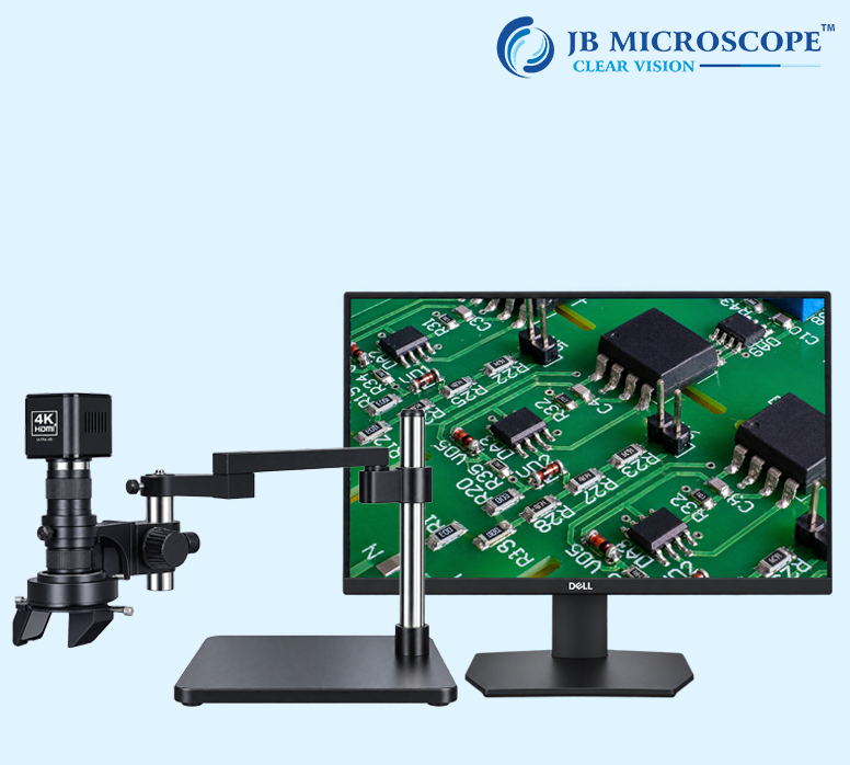
The Monozoom 3D Microscope represents a cutting-edge advancement in microscopy technology, offering a revolutionary approach to scientific exploration and observation. This sophisticated microscope is designed to provide researchers and sci...
The Monozoom 3D Microscope represents a cutting-edge advancement in microscopy technology, offering a revolutionary approach to scientific exploration and observation. This sophisticated microscope is designed to provide researchers and scientists with an immersive three-dimensional experience, allowing for unprecedented insights into the microcosms.
When observing the surface of an object with a microscope, it can be very difficult to determine the shape or topography of the surface since only a small area can be in focus at one time. This is especially true when capturing a photo with a camera. Some digital microscopes have the ability to scan an entire surface and capture each different area that comes into focus, combining them into one fully-focused image. The relative height data from each focal plane can then be used to reconstruct the surface into a 3D image that users can freely manipulate, making it easy to understand the true shape of the surface.
D.F.D. stands for Depth from Defocus. The D.F.D. method calculates three-dimensional depth information based on the amount of defocusing of two-dimensional images. When the lens is shifted vertically towards the target to capture images at different heights, the focus level of an individual point changes gradually. When a position on the target is higher, in a topographical sense, that part of the image will come into focus sooner (when moving the lens downward toward the part). When a position on the target is lower, that part of the image will come into focus as the lens is moved closer to the target. By calculating the height position of the lens when each point in the image comes into focus, a 3D image can be created. Even if perfect focus is unable to be obtained for some areas, the D.F.D. algorithm is still capable of calculating the height location of those pixels and obtaining detailed texture information.
| Parameter | Specification |
|---|---|
| Brand | JB MICROSCOPE |
| Model | JBM-HD3D |
| Zoom Ratio | 1:7 |
| Zoom Objective | 0.7X - 5X |
| Eyepiece | 0.4X |
| Working Distance | 100mm |
| Vertical Post Height | 240mm |
| Vertical Post Diameter | φ32mm |
| Microscope Body Holder | φ50mm |
| Focus Travel | 50mm |
| Base Size | 320x260x16mm (L1 Base) |
| Material | Metal |
| LED-144TP Illuminator Specification | Value |
|---|---|
| Outer Diameter | 100mm |
| Inner Diameter | 61mm |
| Wattage | 4.5W |
| Input Voltage | 90V - 264V |
| Output Voltage | DC 12V |
| Brightness Adjust | 0 - 100% |
| Working Distance | 40 - 250mm |
| Quantity of LED | 144 PCS |
| Brightness | 20000 Lux at height of 100mm |
| Color of Light | 6400K |
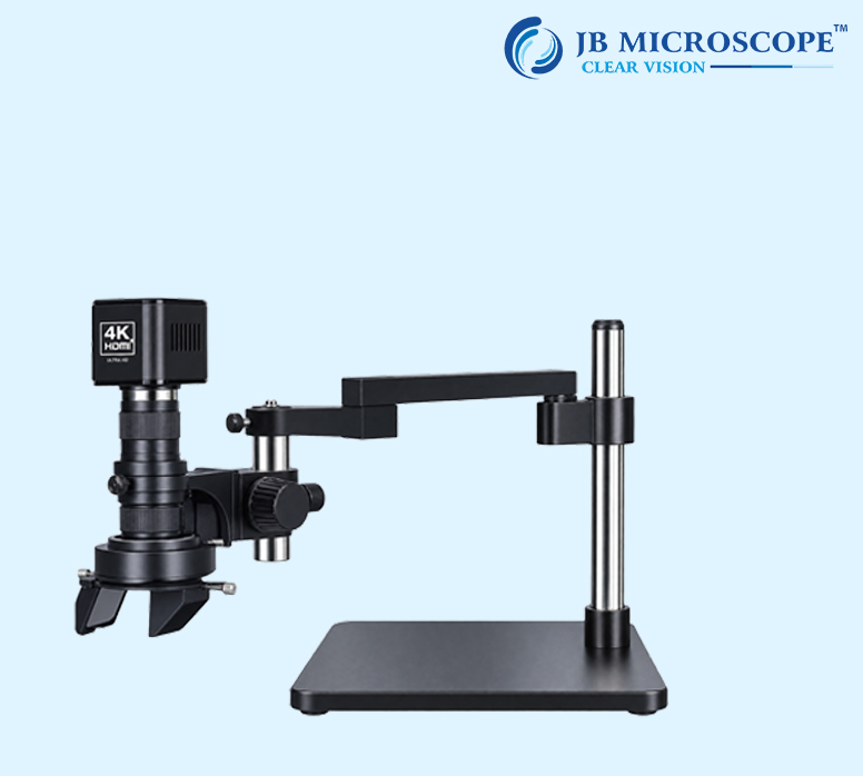
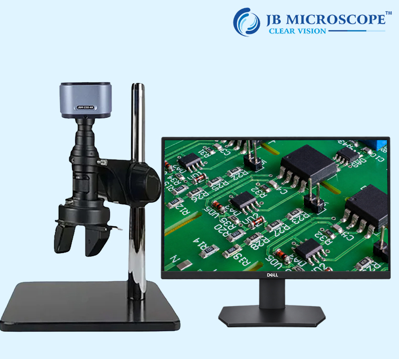
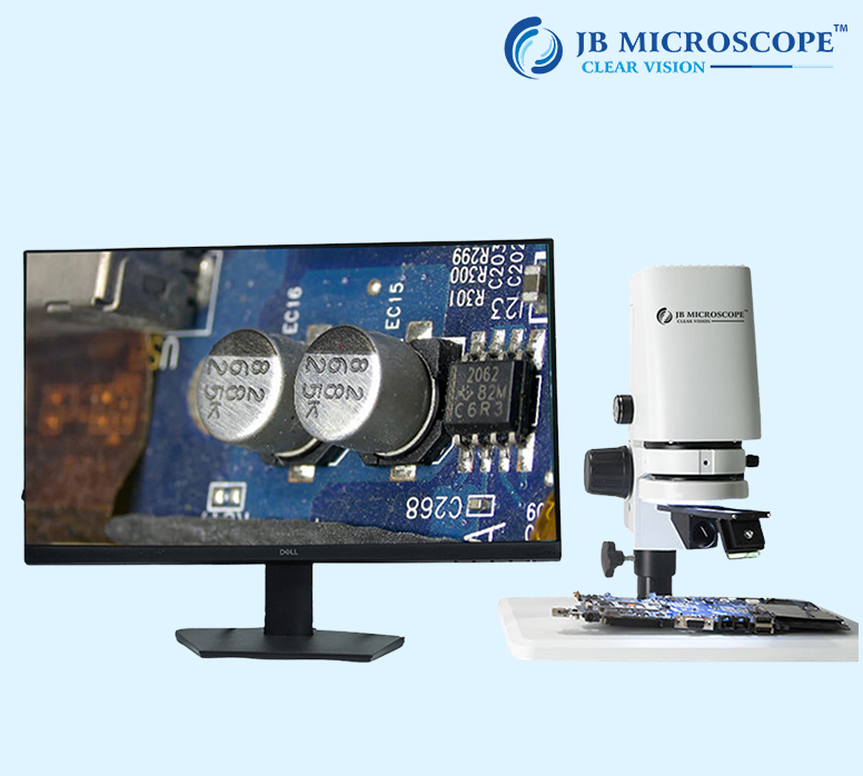
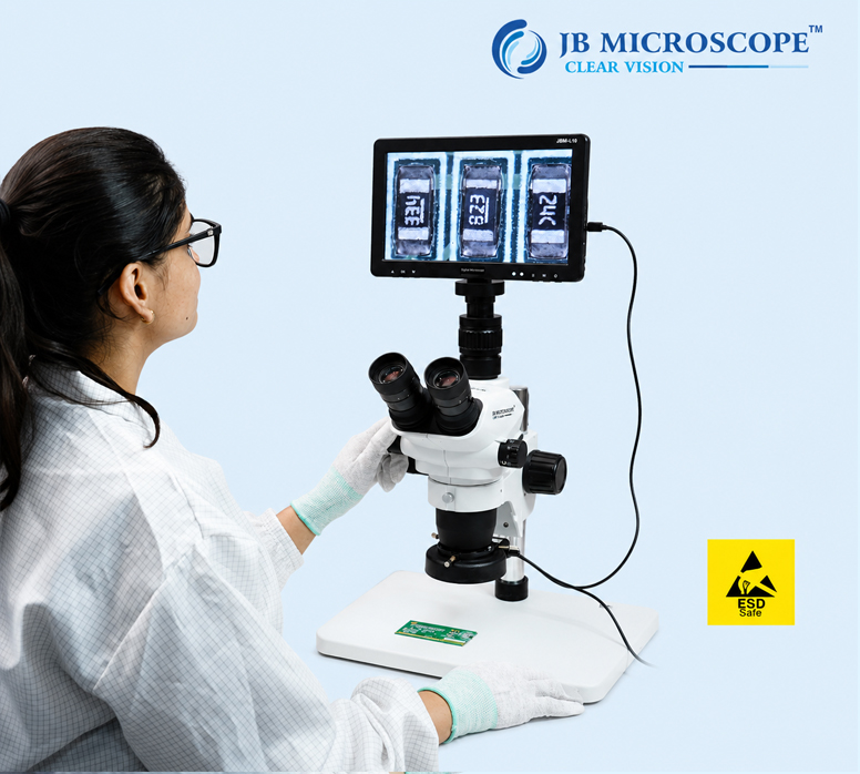
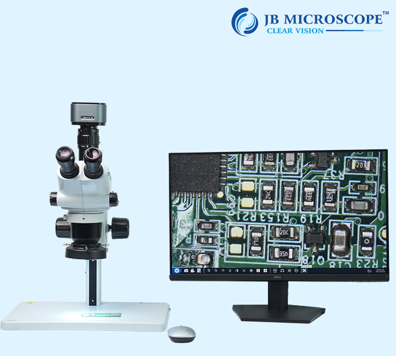
A 3D Microscope in Ambattur Industrial Area, Chennai is an inspection system that helps users view small components, PCBs, solder joints, connectors, mechanical parts, and other objects from different angles. It can be useful when surface height, edges, raised components, and side details need close inspection. JB Microscope offers 3D microscope solutions for electronics, PCB inspection, industrial inspection, assembly, repair, research, and quality control. The JBM-MZ3Di 3D microscope features 0.7X–5X optical zoom, 100 mm working distance, Sony IMX307 CMOS sensor, 1920 × 1080 resolution, an 11.6-inch display, and a 144-LED ring light. Ambattur Industrial Area has many engineering, manufacturing, automotive, electronics, and industrial businesses where detailed inspection of small parts can be important. A 3D microscope can help users inspect components from different viewing angles.
A 3D Microscope can support close inspection of small manufactured components and product details.
It can help inspect PCB components, solder joints, connectors, tracks, and raised parts.
It can support detailed inspection of electronic components during assembly and production.
Suitable systems can be used to inspect small automotive components and electronic parts.
It can be useful for inspecting small mechanical parts, surfaces, edges, and finished products.
Technicians can use different viewing angles while checking components and solder joints.
| Specification | Details |
|---|---|
| Product | 3D Microscope |
| Model Example | JBM-MZ3Di |
| Optical Zoom | 0.7X–5X |
| Working Distance | 100 mm |
| Sensor | Sony IMX307 CMOS |
| Sensor Size | 1/2.8 inch |
| Resolution | 1920 × 1080 |
| Display | 11.6 inch |
| Illumination | 144-LED Ring Light |
| Light Control | Adjustable |
| Focus | Adjustable |
| Viewing | 3D / Different Angles |
| PCB Inspection | Suitable |
| Electronics Inspection | Suitable |
| Industrial Inspection | Suitable |
| Quality Control | Suitable |
Exact specifications depend on the selected model and configuration.
Some components have different heights, raised sections, edges, and side surfaces that may be difficult to inspect from only one direction. A 3D microscope can help users view these areas from different angles.
It can be useful for PCB inspection, electronics repair, soldering, assembly, manufacturing, automotive inspection, engineering, industrial inspection, research, and quality control.
The right model should be selected according to zoom, working distance, camera, display, lighting, and inspection requirements.
A 3D Microscope in Ambattur Industrial Area, Chennai can be useful for manufacturing companies, automotive businesses, electronics units, engineering companies, laboratories, repair centres, research facilities, and quality control departments.
For industrial users in Ambattur, a suitable 3D microscope can support detailed inspection during production, assembly, repair, testing, and final quality checking.
JB Microscope provides microscope solutions for electronics, PCB inspection, automotive inspection, industrial inspection, research, repair, assembly, and quality control.
It is an inspection microscope that helps users view small objects and details from different angles.
Yes. It can inspect PCB components, solder joints, tracks, connectors, and raised parts.
Yes. It can support detailed inspection of small parts and products.
Yes. Different viewing angles can help inspect raised areas and side details.
Yes. It has a 144-LED ring light.
Yes. Suitable setups can be used for small automotive components and electronic parts.
Check zoom range, working distance, camera, display, lighting, viewing angle, and application requirements.
Need a 3D Microscope in Ambattur Industrial Area, Chennai for manufacturing, PCB inspection, electronics, automotive inspection, engineering, repair, or quality control? Contact JB Microscope today to discuss your application and select a suitable 3D microscope system.