Tell us what you need and our team will get back to you with pricing and product details within 2 hours.
Enter your details to connect directly with our technical specialist on WhatsApp.
Quickly find models, categories, and inspection systems across our product catalog.
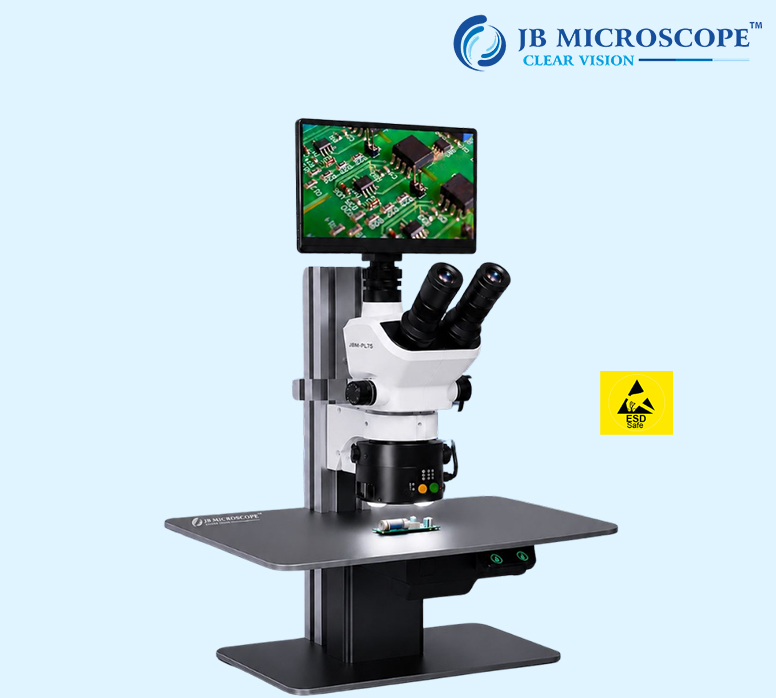
A PCB Inspection Microscope in Mumbai is designed for close inspection of printed circuit boards, electronic components, solder joints, tracks, connectors, and other small parts. It provides an enlarged view that helps technicians and quality teams check PCB details more clearly. JB Microscope offers inspection microscope systems for PCB manufacturing, assembly, electronics repair, soldering, testing, and quality control. Digital camera options can also be added to suitable microscope systems for screen-based viewing and image capture. For buyers in Mumbai, a PCB inspection microscope can be useful in electronics companies, PCB assembly units, repair centers, testing laboratories, manufacturing facilities, and quality control departments.
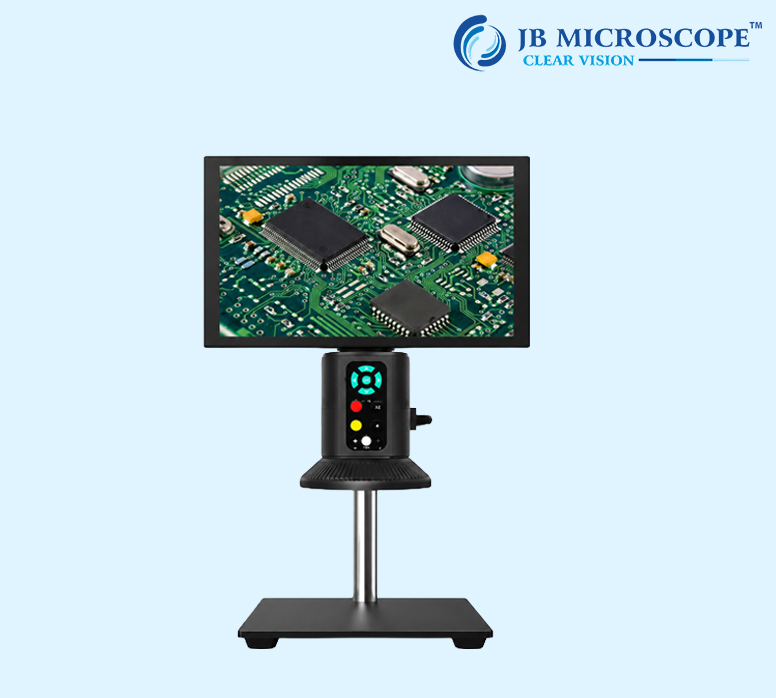
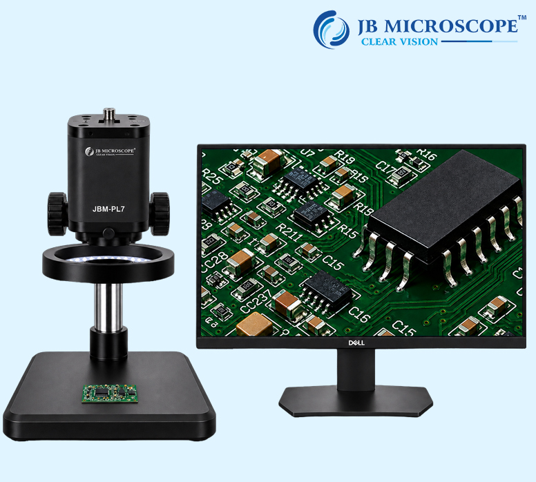
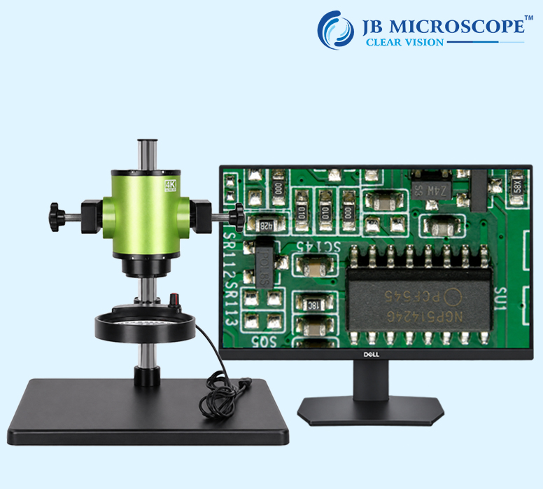
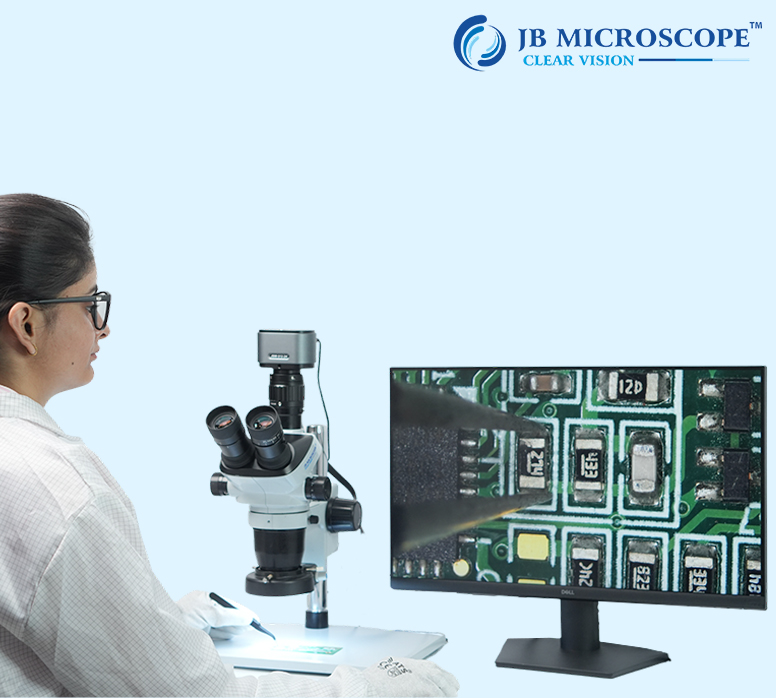
A PCB Inspection Microscope in Mumbai is designed for close inspection of printed circuit boards, electronic components, solder joints, tracks, connectors, and other small parts. It provides an enlarged view that helps technicians and quality teams check PCB details more clearly. JB Microscope offers inspection microscope systems for PCB manufacturing, assembly, electronics repair, soldering, testing, and quality control. Digital camera options can also be added to suitable microscope systems for screen-based viewing and image capture. For buyers in Mumbai, a PCB inspection microscope can be useful in electronics companies, PCB assembly units, repair centers, testing laboratories, manufacturing facilities, and quality control departments.
The working distance is important when technicians need to work on the PCB while viewing it through the microscope. A suitable setup can provide enough space for soldering, repair, and other tasks.
A PCB Inspection Microscope can help manufacturers check boards during production. Components, tracks, solder points, and connections can be viewed closely.
It can be used to check component placement, soldering, and connections after assembly.
Technicians can use the microscope to find damaged components, poor solder joints, broken connections, and other visible problems.
The enlarged view can help technicians work with small soldering points and electronic components during rework.
Quality teams can use the microscope to check PCB assembly and identify small visible defects before the product moves to the next stage.
A microscope can support close visual checking before or after electronic testing.
| Specification | Details |
|---|---|
| Product | PCB Inspection Microscope |
| Microscope Type | Digital / Stereo Inspection Microscope |
| Main Use | PCB Inspection |
| Viewing | Optical / Digital |
| Magnification | Model Based |
| Zoom | Model Based |
| Working Distance | Model Based |
| Camera | Model Based |
| Camera Resolution | Model Based |
| Display | Model Based |
| Lighting | LED |
| Focus | Adjustable |
| Image Capture | Model Based |
| Video Recording | Model Based |
| PCB Inspection | Suitable |
| Solder Inspection | Suitable |
| Electronics Repair | Suitable |
| Quality Control | Suitable |
Note: JB Microscope offers different PCB inspection microscope configurations. Exact magnification, working distance, camera resolution, display, lighting, and other technical details depend on the selected model.
PCBs contain many small components, tracks, and solder connections. These details can be difficult to inspect with normal eyesight. A microscope provides an enlarged view and makes close checking easier.
A digital microscope setup can display the PCB image on a screen. This can help technicians work more comfortably and can also allow images or videos to be captured on supported systems.
For buyers in Mumbai, select the microscope according to the PCB size, component size, required magnification, working distance, camera, lighting, and type of inspection.
A PCB Inspection Microscope in Mumbai can be useful for PCB manufacturers, electronics companies, assembly units, repair centers, testing laboratories, engineering businesses, and quality control teams.
Mumbai and nearby industrial areas have many electronics and manufacturing businesses where close PCB inspection can be an important part of production and repair.
JB Microscope provides microscope solutions for PCB inspection, electronics repair, industrial inspection, research, and quality control.
A PCB Inspection Microscope is used to enlarge and inspect small details on printed circuit boards, including components, tracks, solder joints, and connections.
Yes. It can help technicians inspect small components and soldering points during PCB repair and rework.
Yes. A suitable microscope can provide a close view of solder joints and small connection points.
Yes. It can help quality teams check PCB components, soldering, connections, and visible defects.
Yes. Selected microscope systems can be connected to suitable microscope cameras for digital viewing and image capture.
Check the required magnification, working distance, camera, lighting, display, PCB size, and type of inspection before choosing a model.
If you need a PCB Inspection Microscope in Mumbai for PCB manufacturing, assembly, electronics repair, solder inspection, testing, or quality control, choose a model according to your work requirements. A suitable microscope can provide a clear enlarged view and make detailed PCB inspection easier.