Tell us what you need and our team will get back to you with pricing and product details within 2 hours.
Enter your details to connect directly with our technical specialist on WhatsApp.
Quickly find models, categories, and inspection systems across our product catalog.
A 3D Microscope in Noida is a useful inspection system for viewing small components, electronic parts, PCBs, solder joints, connectors, and other fine details from different angles. It can help users check the top, sides, edges, and raised areas of an object without moving the sample again and again. JB Microscope offers 3D microscope solutions for electronics inspection, PCB inspection, industrial work, repair, assembly, research, and quality control. Different models can be selected according to magnification, camera quality, working distance, lighting, and viewing needs. Noida has many electronics, engineering, manufacturing, assembly, and technology companies. A 3D microscope can support detailed inspection work in these industries where small parts need to be checked carefully.
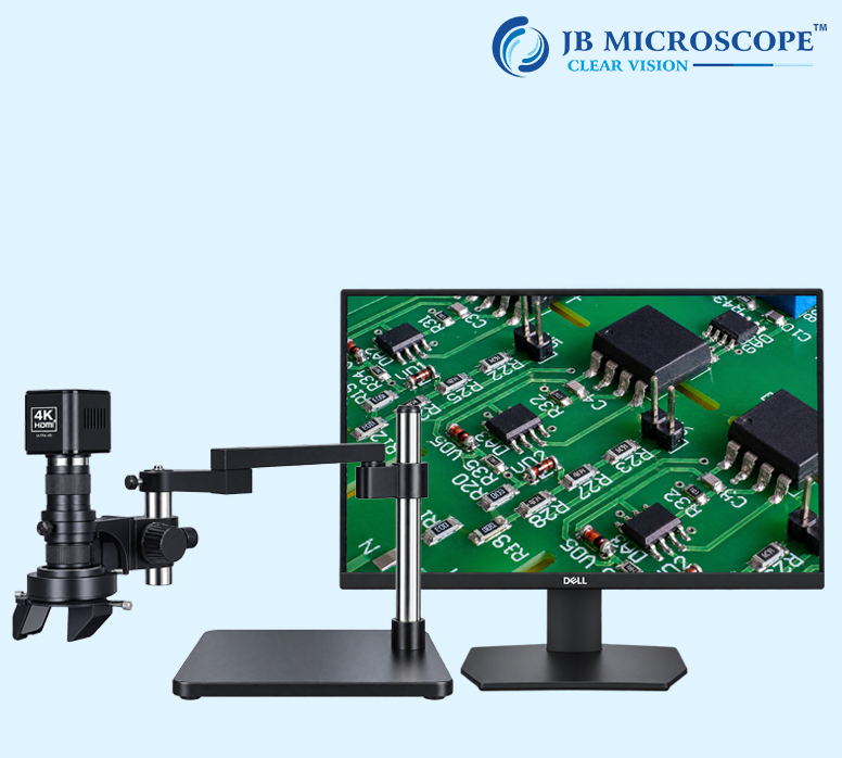
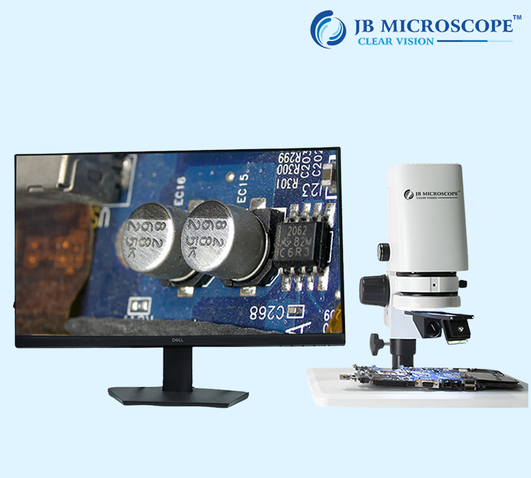
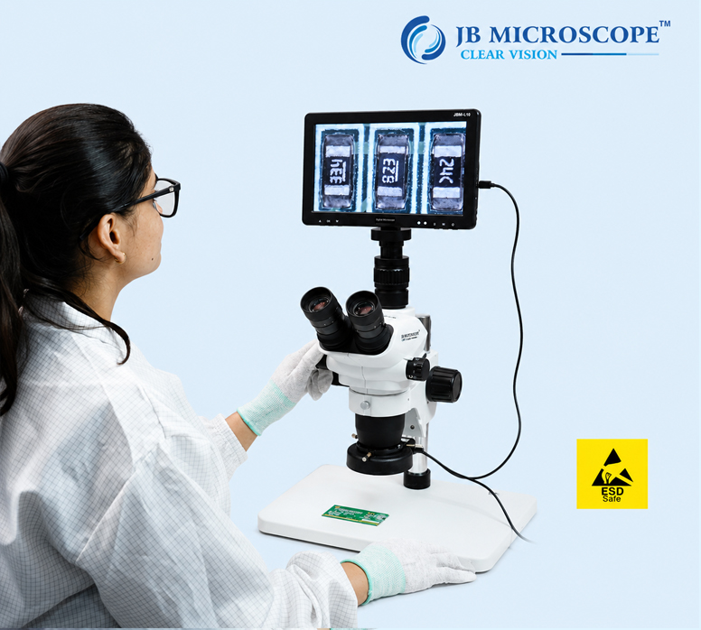
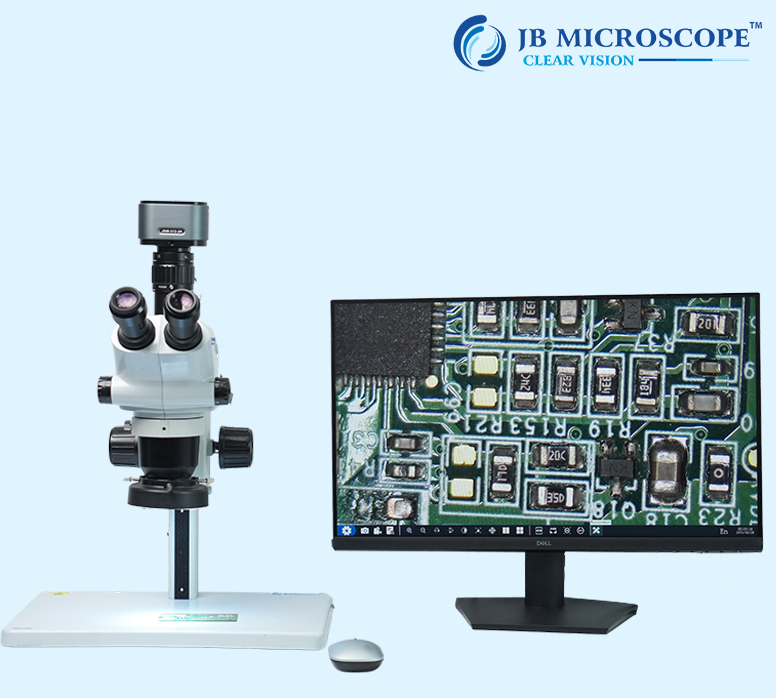
A 3D Microscope in Noida is a useful inspection system for viewing small components, electronic parts, PCBs, solder joints, connectors, and other fine details from different angles. It can help users check the top, sides, edges, and raised areas of an object without moving the sample again and again. JB Microscope offers 3D microscope solutions for electronics inspection, PCB inspection, industrial work, repair, assembly, research, and quality control. Different models can be selected according to magnification, camera quality, working distance, lighting, and viewing needs. Noida has many electronics, engineering, manufacturing, assembly, and technology companies. A 3D microscope can support detailed inspection work in these industries where small parts need to be checked carefully.
The 3D viewing system can help users inspect different sides of a component while keeping the sample in place. This can be useful for raised PCB components, connectors, solder joints, edges, and small industrial parts.
A 3D Microscope can help users inspect PCB components, solder joints, tracks, connectors, and raised parts on circuit boards.
It can be used to check small electronic components, wires, connectors, and other parts from different viewing angles.
Technicians can use the microscope to inspect small components and soldering areas during repair and rework.
Manufacturers can use a 3D microscope to check small machine parts, surfaces, edges, and other product details.
It can help users inspect component placement, connections, and small assembly details.
Quality teams can use the microscope to check small parts and visible defects from different angles.
| Specification | Details |
|---|---|
| Product | 3D Microscope |
| Microscope Type | Digital 3D Inspection Microscope |
| Viewing | Digital Screen |
| Camera | Digital CMOS Camera |
| Sensor | Model Based |
| Resolution | Model Based |
| Magnification | Model Based |
| Zoom | Model Based |
| Working Distance | Model Based |
| Rotary Viewing | Available on Suitable Models |
| Display | Model Based |
| Lighting | LED Ring Light |
| Brightness Control | Adjustable |
| Focus | Adjustable |
| Image Capture | Model Based |
| Video Recording | Model Based |
| PCB Inspection | Suitable |
| Electronics Inspection | Suitable |
| Industrial Inspection | Suitable |
| Quality Control | Suitable |
Note: Exact camera resolution, magnification, zoom range, working distance, display, frame rate, lighting, and rotary viewing features depend on the selected JB Microscope model.
Some small components have sides, edges, raised areas, and surfaces that may be difficult to inspect from one fixed position. A 3D microscope gives users more viewing angles and can make these areas easier to check.
It can be useful for PCB inspection, electronics repair, soldering, assembly, industrial inspection, and quality control. Digital models can also display the enlarged image on a screen, allowing users to inspect the sample more comfortably.
On supported models, images and videos can be captured for inspection records, training, reports, and future reference.
For buyers in Noida, choose the microscope according to the sample size, required magnification, working distance, camera quality, lighting, display, and inspection purpose.
A 3D Microscope in Noida can be useful for electronics manufacturers, PCB assembly companies, engineering units, repair centers, laboratories, assembly facilities, and quality control departments.
Noida has a strong base of electronics, technology, engineering, and manufacturing businesses. Detailed inspection can be important during production, assembly, repair, testing, and quality checking.
JB Microscope provides microscope solutions for PCB inspection, electronics, industrial inspection, repair, research, assembly, and quality control applications.
A 3D Microscope is an inspection system that helps users view small objects and their details from different angles.
Yes. It can be used to inspect PCB components, solder joints, tracks, connectors, and raised parts.
Yes. It can help technicians view small components and soldering areas during repair and rework.
It allows users to inspect different sides, edges, and raised areas of a component without repeatedly changing its position.
Yes, depending on the selected microscope model, camera, and software features.
Check the magnification, zoom, working distance, camera resolution, lighting, display, viewing angle, and type of inspection before selecting a model.
If you need a 3D Microscope in Noida for PCB inspection, electronics, repair, assembly, industrial inspection, research, or quality control, choose a model according to your actual work requirements. A suitable 3D microscope can provide clear digital viewing and make inspection of small components easier from different angles.